
리뷰목적
- Sapphire Rapirs Architecture Rapids Analysis
- Basic SPEC
- SPR Category
- D2D interface, MDFIO 분석 (expected) - [DONE]
- Power density
- BW Density
- Protocol
- DL Boost technology - [DONE]
- AVX
- AMX
- Computation Power, TOPS.
- Mesh interconnect BW/Bit-width - [TBD]
- Memory system - [TBD]
- Inference 시장 및 SPR/EMR 침투가능성 분석 - [TBD]
1. Sapphire Rapids Architecture Analysis
Basic SPEC [1]
- 19.828mm x 20.190mm (400.33mm2)
- Monolithic or 4 die manufactured on Intel 7 process technology
- #of Cores: 8~60 (x2 threads)
- Base clk 1.8~3.6Ghz / All core turbo boost 1.9~4Ghz / Max turbo boost 1.9~4.1Ghz
- 20~110MB L2/3 Cache
- TDP ~200W, ~300W, Max 350W
- 8 DDR5 channels 4000/4400/4800MT/s, Max 4TB Capacity
- 4 HBM2E channels, 64GB
- 32GT/s PCIe(gen5)/CXL, Lanes x16/x8, Max 80 channels
- 16GT/s UPI 0/2/3/4channels
- EMIB D2D Interface Aggregated 10TB/s bandwidth
- Soket Level Scalability per server(motherboard): 1S,2S,8S
- $400, $600, ~ $10,000, $17,000(w/ HBM)
- Integrated accelerators (관심있는 것만)
- IAA : In-memory Analytic Accelerator, Intel query processing lib.
- DSA : Data Streaming Accelerator, Storage Perf Dev Kit(SPDK), Data Plande Deb Kit(DPDK)
- QAT : Quick Assist Technology, QATzip, OpenSSL, boring SSL.
- DLB : Dynamic Load Balancer, VPP IPSec, Data Plane DevKit(DPDK)
- …

SPR Server Category
- SPR server은 $400~$17000에 이르기까지 다양한 제품군을 지원[3]. 아래 카테고리는 위키피디아[4]에서도 찾아볼 수 있음.
- 위키피디아를 다시 열어보니, 약간의 업데이트가 되었음 특히 XCC,MCC에 대한 정보가 가려졌음.
- 아래 정보를 참고하면 4410T의 경우 IOT향이라는 것 같은데, 이것은 왜 SERVER 카테고리에 들어있는 지 모르겠음. 그렇다고 Workstation도 아니고, Edge category를 하나 신설해야 하는 것 아닌 지.

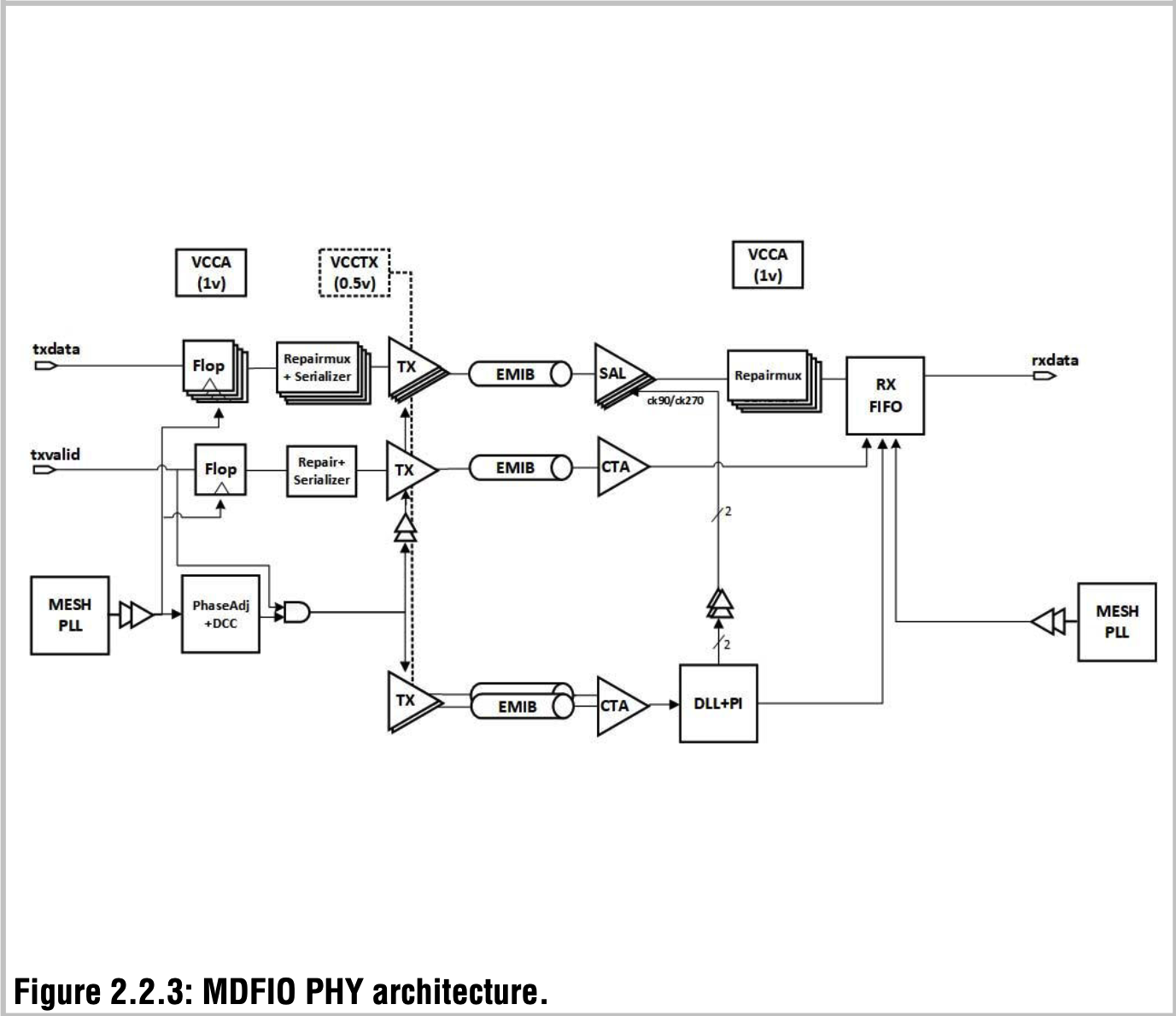
Multi-Die Fabric IO(MDFIO) [1]
- EMIB/MDF PHYs
- 40Blocks, 10 EMIB Blocks per die[2]
- Each MDF = 2 EMIB Blocks
- 0.5pJ/bit w/ VCCTX0.4V
- UCIe standard 수준
- Handling on-die dynamic voltage frequency scaling(DVFS from 800Mhz to 2.5Ghz)
- MDFIO와 무슨 상관이 있는 것인 지 모르겠음.
- Bandwidth 500GB/s per crossing, accross 20 crossings, 10TB/s aggregate D2D BW
- 10 set MDF -> MDF 1개당 Bi 1TB/s(10TB/s / 10set) -> MDF 1개당 Tx 512GB/s, Rx 512GB/s
- 5 MDF per die = 10 EMIB block per die ->1 MDF = 2 EMIB block -> EMIB block 1개당 Tx 256GB/s, Rx 256GB/s
- EMIB block 2개 = 1 MDF = 2 crossing = one-way 500GB/s
- Raw-wire BER 1e-27(1e+27개당 1개 error) to achieve a FIT of <1(10억 시간 당 1번 고장) and avoid the need for in-line correction or replay to allow <10ns round trip latency.
- 1.6G to 5.0GT/s parallel signaling
- Lane속도와 BW를 알고 있으니, MDFIO하나의 TX/RX lane개수를 구해보려고 하는데, 여기서 계산이 뭔가 좀 미심쩍음.
- EMIB block lane = 256GB/s / 5GT/s = 410개(one-way).
- EMIB block 내 module이 4개 있다고 해도 모듈당 TX 100개/Rx 100개임.
- UCIe standard 는 stacking해서 x32.
- Source-synchronous clocking with DLL and PIs for training on the RX side.
- Low-swing double-data-rate N/N transmitter for reduced power with AC-DBI for power supply noise reduction
- Strongarm latch receiver with VREF training
- Offset cancellation directly connected on the Rx bump
- Lane repair to recover defects pre and post assembly.
SPR MDFIO(EMIB) 성능분석 중간 결론
MDFIO Beachfront size = 5.764mm
MDFIO BW Density = 1TB/s / 5.764mm = 0.173TBps/mm = 1.388Tbps/mm
(cf. UCIe Standard 0.9Tbps/mm, UCIe Advanced 5.2Tbps/mm)
**Power density는 0.5pJ/bit으로 UCIe standard와 같고,**
**Bandwidth density는1.4Tbps/mm로 UCIe standard(0.9Tbps/mm)보다 조금 나은 정도.**
EMIB PHY라 불리는 SPR의 D2D interface IP는, Energy efficiency/BW Density를 고려해 봤을 때, UCIe Standard 수준으로 파악됨.
UCIe standard 수준의 BW Density로 10TB/s per whole SPR(5TB/s per die)의 BW를 확보하려다 보니, EMIB의 크기가 지나치게 커지게 됨.
(설마, SPR Core floor plan을 마치고, 빈 공간 없이 Beach front에 EMIB를 배치하다보니, 많이 배치하게 되었을까?)SPR을 한참 개발할 때에는 Advanced packaging 기술이 아직 도입단계였기 때문에 Standard 수준의 BW density가 최선이었을 수는 있음.
낮은 BW Density는 D2D interface block의 Area overhead 증가시킴.
Intel은 SPR의 다음 버전인 EMR에서 이 Area overhead를 줄이기 위해서, D2D Chiplet 개수를 2개로 줄인다고 함. [7]
그러나, 이제는 UCIe-ADV 혹은 비슷한 수준의 BW density를 갖는 다른 D2D Interface(OHBI, in-house)를 채택하는 것도 가용한 방법이었을텐데 EMR에서 단순히 chiplet을 2개로 줄인 것에 의문이 듦. Glass core substrate와 Co-packed optics의 Intel에서 발표한 Next packaging tech를 통해[5] 더 큰 단위에서의 Scaleout이 Cost측면에서 유리하다고 봤을 수도 있을 것 같음. Google TPUv4에서 주장하는 바 처럼[6].
DL boost Technology
DL Boost Technology is a marketing name for instruction set architecture features on the x86-64 designed to improve performanced on deep learing tasks.
DL Boost Instruction extends + data type.
- AVX-512 FP32 FP64
- AMX INT8(inference), BF16(Training/inference)
- AMX-FP16
- AMX-COMPLEX supports FP16 complex number, where a pair of adjacent FP16 numbers represent real and imaginary parts of the complex number.
- ... 많이 있지만 당장 관심있는 것은 AMX이므로, DL boost technology에 해당하는 Instruction extend정리 보류.
AMX는 INT8/BF16/FP16/복소수(Complex)의 Precision을 지원함.
(AMX : Built-in Dedicated acclerator hardware block found on each CPU core to optimize deep learning training and inference workloads.)
AMX uARCH는 아래 2개의 구성으로 이루어져 있음

- Register file consists of 8 tiles, each with 16 rows of size of 64 bytes (32 BF16/FP16, 64 INT8)
- Only matrix multiplication is support
- Operation/cycle
- AMX-INT8 : 16(rows) x 64(Bytes) x 2(ops) = 2048
- AMX-BF16 : 16(rows) x 32(Bytes) x 2(ops) = 1024
- SPR Computation Power
- SPR_SP (Server, only for XCC, multi die) --> Max 356.3TOPS
- Total Cores: 16~60 → 60 선택 (8490H)
- (= #of AMX)(4Tiles(chiplet) x 4Cores/Tile ~ 4Tiles x 15Cores/Tile) [1]
- Core당 AMX가 1개 존재하는 것인 지, 맞는 것 같기는 한데, 추후 확인 필요.
- Clock frequency [1] : All core turbo 2.9Ghz(8490H) 선택
- Base frequency: 3.6~1.9 Ghz
- All Core Turbo Clk Freq: 3.2~2.9 Ghz
- Max Turbo Clk Freq: 1.9~4.1 Ghz
- AMX INT8 2048 operation/cycle [2, 3]
- SPR 104.8 ~ 356.3TOPS / Max 112MB L2 / Max 112.5MB L3 / Max 4TB w/ DDR5 + HBM2e / 350W / $4,234 ~ $17,000
- Total Cores: 16~60 → 60 선택 (8490H)
- SPR_WS (Workstation) --> Max 550.5 TOPS
- Xeon w9 3495x Core 56
- Clk freqeuncy 1.9~4.8Ghz
- AMX INT8 Ops 2,048
- 229.3~550.5 TOPS@INT8
- SPR_SP (Server, only for XCC, multi die) --> Max 356.3TOPS
SPR Computation Power 중간결론
INT8기준 서버향과 워크스테이션향 boost clk freq 동작 가정 시 Computation power는 아래와 같다.
SPR_SP MAX 356.3TOPS @INT8
SPR_SP MAX 128FLOPS@BF16(FP16)
SPR_WS MAX 550.5TOPS @INT8
SPR_WS MAX 275FLOPS@BF16(FP16)
CPU에서 지원해줄 수 있는 INT8 Inference computation power로는 매우 높은 성능인 듯.
Computation power, Memory BW, Memory Capacity 의 3가지 기준으로 CPU vs NPU를 비교해 봤을 때, SPR의 뚜렷한 단점이 보이지 않음.
다만, 실제 Workload를 돌려보면서 전성비(TOPS/W)와 Effective TOPS 평가가 있어야 더 의미있는 비교가 가능 할 듯.
Additional Analysis for Power Efficiency
1) NPU의 일반적인 TOPs/W = 2TOPS/w
2) SPR의 TDP기준 TOPS/W = 550.5/350 = 1.57TOPS/w
1번은 Effect/Consumed power이고, 2번은 TDP라는 점에서 괴리가 있지만, TDP를 절반으로 깎는다고 해도, 어느정도의 성능은 확보되는 것으로 판단됨.
TODO1) AI 서비스 관점에서 CPU외 가속기로 Inference workload offloading을 하는 것의 overhead나 gain이 얼마나 될 지.이전에 넘겨듣기로 실제 AI서비스에서 AI알고리즘 동작이 차지하는 시간비중은 20%도 되지 않는다고 들었음. 이 부분에 대한 research가 필요함.
Mesh Interconnect SPEC
TBD
Memory Subsystem SPEC
HBM + DDR5
CXL 활용 방안, (CXL?)
2. HPC Inference Market Penetration Probability and Penetration Rate of SPR
Questions
[Q1] 아래 MDFIO PHY Architecture와 UCIe v1.1 SPEC PHY Architecture 비교시, 가장 크게 다른 점은 DLL/PI가 Tx에 있는 지(UCIe) Rx에 있는 지(SPR)인 것 같은데, 어떤 차이가 있는 지 모르겠음.

[Q2] SPR block repair/recovery methods (TBD: 잘 모름, 그대로 옮겨 적어 놨음.)
- A combination of muxes and IO signals allow the test and debug fabrics to operate within a die or utilize the EMIB to enable a D2D data-path on assembled parts.
- A parallel test interface is accessible via DDR channels, a single die provides scan data via packetized test data, to access IPs on an asembled 4-die part.
- Parallel test of re-instantiated IPs on all four die is supported with a single set of patterns in tester memory along with test failure information to support recovery.
- A parallel trace interface is available via dedicated GPIO to allow access to debug dtat from any of the 4 individual dies.
- JTAG is implemented as single controller for system view, but four indivifual controllers for high volume manufacturing access.
TODO
TODO1) AI 서비스 관점에서 CPU외 가속기로 Inference workload offloading을 하는 것의 overhead나 gain이 얼마나 될 지.이전에 넘겨듣기로 실제 AI서비스에서 AI알고리즘 동작이 차지하는 시간비중은 20%도 되지 않는다고 들었음. 이 부분에 대한 research가 필요함.
References
[1] ISSCC22 Sapphire Rapids: The Next-Generation Intel Xeon Scalable Processor
https://ieeexplore.ieee.org/stamp/stamp.jsp?tp=&arnumber=9731107
[2] Intel Emerald Rapids Backtracks on Chiplets – Design, Performance & Cost
유료 구독 서비스 매체이지만, 어느정도는 읽을 수 있음.
https://www.semianalysis.com/p/intel-emerald-rapids-backtracks-on


[3] WCCFTECH "Intel 4th Gen Xeon CPUs Official: Sapphire Rapids With Up To 60 Cores, 112.5 MB Cache, 8-Socket Scalability, 350W TDP, Top SKU At $17,000 US" 23/01/10
4th Gen Xeon Scalable processors codenamed Sapphire Rapids offer (vs 3rd Gen Xeon CPUs)
- +53% Average Performance Gain in General Purpose Computing
- Up To 10x High inference & training performance in Artificial Intelligence
- Up To 2x capacity for vRAN workloads at the same power envelope (Network 5G vRAN)
- Up To 2x higher data compression with 95% fewer cores (Networking & Storage)
- Up To 3x higher performance in Data Analytics
- Up To 3.7x performance on memory-bound workloads in HPC (Xeon Max CPU Series)
관심있는 사항은 2, 4번 항목. 2번은 3rd Gen에서 AMX가 없었으니, 10배 빨라지는 것은 당연한 이야기 일 듯 하고. 4번은 Mesh interconnect구조에서 AI Inference향 동작시 Compression이 얼마나 잘 되고, 그게 networking traffic efficiency에 어떤 도움이 되는 지.
All the Built-In Accelerators and Security Engines
- Intel Advanced Matrix Extensions (AMX)
- Intel QuickAssist Technology (QAT)
- Intel Data Streaming Accelerator (DSA)
- Intel Dynamic Load Balancer (DLB)
- Intel In-Memory Analytics Accelerators (IAA)
- Intel Advanced Vector Extensions 512 (AVX-512)
- Intel Advanced Vector Extensions 512 (AVX-512) for vRAN
- Intel Crypto Acceleration
- Intel Speed Select Technology (SST)
- Intel Data Direct I/O Technology (DDIO)
- Intel Software Guard Extensions (SGX)
- Intel TrustDomain Extension (TDX)
- Intel Control-Flow Enforcement Technology (CET)
관심있는 항목은 1,3,4,5,6,7.
[4] Sapphire Rapids Wikipedia
https://en.wikipedia.org/wiki/Sapphire_Rapids
[5] Intel's Process Roadmap to 2025: with 4nm, 3nm, 20A and 18A?!
[6] TPU v4: An Optically Reconfigurable Supercomputer for Machine Learning with Hardware Support for Embeddings
https://arxiv.org/ftp/arxiv/papers/2304/2304.01433.pdf
[7] Intel Emerald Rapids Backtracks on Chiplets – Design, Performance & Cost
https://www.semianalysis.com/p/intel-emerald-rapids-backtracks-on
[8] Intel Solution Brief Document. Accelerate Artificial Intelligence (AI) Workloads with Intel Advanced Matrix Extensions (Intel AMX
Materials
https://fuse.wikichip.org/news/6119/intel-unveils-sapphire-rapids-next-generation-server-cpus/
Intel Unveils Sapphire Rapids: Next-Generation Server CPUs
Intel unveiled Sapphire Rapids, its next-generation server CPUs
fuse.wikichip.org
Intel Xeon Sapphire Rapids: How To Go Monolithic with Tiles
One of the critical deficits Intel has to its competition in its server platform is core count – other companies are enabling more cores by one of two routes: smaller cores, or individual chiplets connected together. At its Architecture Day 2021, Intel h
www.anandtech.com
4th Gen Intel Xeon Processor Scalable Family, sapphire rapids
A technical overview of the 4th Gen Intel® Xeon® Processor Scalable Family based on the formerly codenamed Sapphire Rapids architecture.
www.intel.com

https://download.intel.com/newsroom/2021/client-computing/intel-architecture-day-2021-fact-sheet.pdf

https://www.phoronix.com/review/intel-xeon-amx/2
Intel Advanced Matrix Extensions [AMX] Performance With Xeon Scalable Sapphire Rapids - Phoronix
At this early stage of software maturity around Advanced Matrix Extensions, the most notable user of it is Intel's own oneDNN library. Intel's oneAPI Deep Neural Network Library (oneDNN) provides optimized implementations of "deep learning building blocks"
www.phoronix.com
Intel Launches Sapphire Rapids Fourth-Gen Xeon CPUs and Ponte Vecchio Max GPU Series
Intel pushes up to 60 cores.
www.tomshardware.com


https://www.techpowerup.com/292204/intel-sapphire-rapids-xeon-4-tile-mcm-annotated
Intel "Sapphire Rapids" Xeon 4-tile MCM Annotated
Intel Xeon Scalable "Sapphire Rapids" is an upcoming enterprise processor with a CPU core count of up to 60. This core-count is achieved using four dies inter-connected using EMIB. Locuza, who leads social media with logic die annotation, posted one for "S
www.techpowerup.com
'Study > Computer System' 카테고리의 다른 글
| [Intel Sapphire Rapids] AMX (0) | 2023.05.08 |
|---|---|
| [Review][Article] Chiplet Summit: Challenges of Chiplet-Based Designs (0) | 2023.02.08 |